| CPC H05K 1/0206 (2013.01) [H01L 23/4985 (2013.01); H01L 23/49838 (2013.01); H01L 24/17 (2013.01); H05K 1/189 (2013.01); H01L 24/16 (2013.01); H01L 2224/16225 (2013.01); H01L 2224/17519 (2013.01)] | 16 Claims |
|
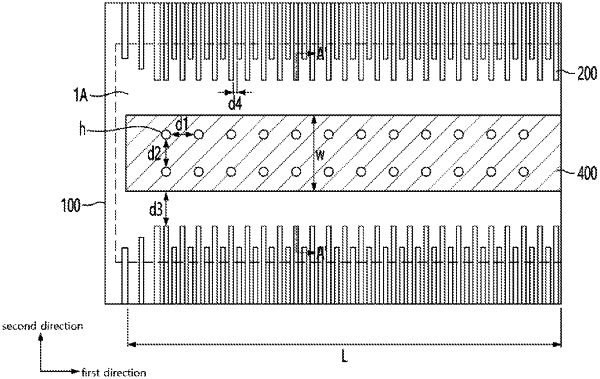
1. A flexible circuit board for a chip on film, the flexible circuit board comprising:
a substrate including a first surface and a second surface opposite to the first surface, and the substrate including a chip mounting region;
a circuit pattern layer disposed on the first surface; and
a heat dissipation part disposed on the chip mounting region,
wherein the substrate is formed with at least two or more holes that are provided in a region overlapping the heat dissipation part, and
the heat dissipation part includes:
a heat dissipation pattern layer disposed on the first surface;
a connection layer disposed inside the hole; and
a heat dissipation layer disposed on the second surface,
wherein a first direction corresponds to a longitudinal direction of a chip disposed on the chip mounting region, and a second direction corresponds to a width direction of the chip disposed on the chip mounting region,
wherein a first separation distance is a spaced apart distance in the first direction of two of the holes, a second separation distance is a spaced apart distance in the second direction of two of the holes, and the first separation distance is smaller than the second separation distance,
wherein a third separation distance is a minimum separation distance in the second direction of the heat dissipation pattern layer and the circuit pattern layer, and the third separation distance is greater than the second separation distance,
wherein the circuit pattern layer has a plurality of circuit patterns,
wherein a fourth separation distance is a minimum separation distance between two adjacent circuit patterns of the plurality of circuit patterns, and the fourth separation distance is smaller than the first separation distance.
|