| CPC H04W 72/23 (2023.01) [H04L 5/003 (2013.01); H04L 5/0037 (2013.01); H04L 5/0044 (2013.01); H04L 5/0051 (2013.01); H04L 5/0055 (2013.01); H04L 5/0094 (2013.01); H04W 72/1273 (2013.01); H04W 72/0446 (2013.01); H04W 72/12 (2013.01)] | 20 Claims |

|
11. An apparatus, comprising:
a memory; and
one or more processors coupled to the memory, the one or more processors and the memory being configured to:
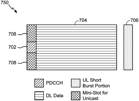
be scheduled to receive first data in a control portion, the control portion comprising a number of symbols in a slot, the control portion comprising a frequency band utilized for control information;
be scheduled to receive second data in a second portion of the slot, the second portion of the slot being outside of the number of symbols, the first data and the second data being received on a second frequency band;
transmit an acknowledgement to acknowledge both the first data and the second data.
|