US 11,902,408 B2
Systems and methods for symbol-spaced pattern-adaptable dual loop clock recovery for high speed serial links
Gaurav Malhotra, Cupertino, CA (US); Amir Amirkhany, Sunnyvale, CA (US); and Jalil Kamali, San Jose, CA (US)
Assigned to Samsung Display Co., Ltd., Yongin-si (KR)
Filed by Samsung Display Co., Ltd., Yongin-si (KR)
Filed on Dec. 9, 2022, as Appl. No. 18/078,631.
Application 18/078,631 is a continuation of application No. 17/508,898, filed on Oct. 22, 2021, granted, now 11,546,127.
Claims priority of provisional application 63/227,605, filed on Jul. 30, 2021.
Claims priority of provisional application 63/162,883, filed on Mar. 18, 2021.
Prior Publication US 2023/0104142 A1, Apr. 6, 2023
This patent is subject to a terminal disclaimer.
Int. Cl. H03D 3/18 (2006.01); H03D 3/24 (2006.01); H04L 7/00 (2006.01); H03L 7/08 (2006.01)
CPC H04L 7/0016 (2013.01) [H03L 7/0807 (2013.01)] 20 Claims
OG exemplary drawing
 
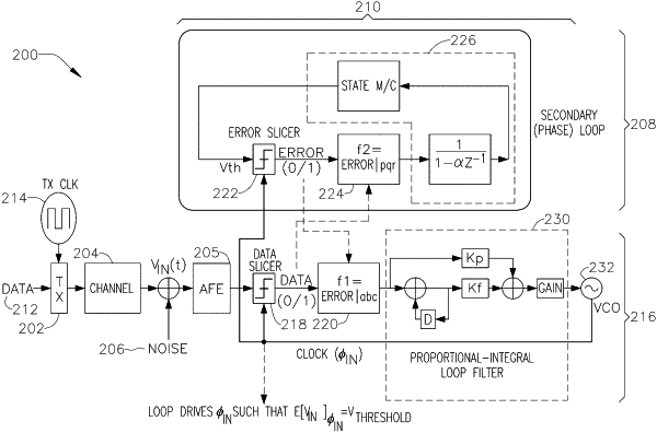
1. A circuit, comprising:
a data slicer configured to output data values based on an input signal;
a first error block; and
a phase adjustment loop, comprising:
a first error slicer configured to generate a first error signal based on a threshold voltage and an input voltage, wherein the first error block is configured to selectively output the first error signal in response to a first pattern in the output data values;
a second error block configured to selectively output the first error signal in response to a second pattern in the output data values; and
a voltage threshold modification circuitry configured to adjust the threshold voltage based on output of the second error block.