| CPC H04L 25/03057 (2013.01) [H03K 5/133 (2013.01); H03K 17/6871 (2013.01)] | 8 Claims |

|
1. An apparatus, comprising:
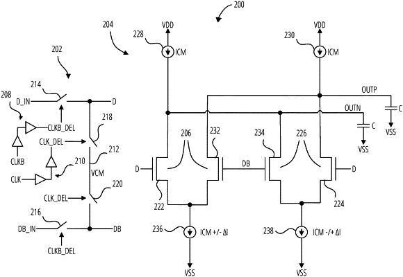
a first electrically controllable switch to receive a history bit and selectively provide the history bit as a delayed history bit to gate terminals of first transistors of a decision feedback equalization (DFE) tap circuitry;
a second electrically controllable switch to receive a complementary history bit and selectively provide the complementary history bit as a delayed complementary history bit to gate terminals of second transistors of the DFE tap circuitry;
one or more delay elements to provide one or more delayed data integration clock signals responsive to one or more data integration clock signals that indicate a start of a data integration state, a complementary delayed data integration clock signal of the one or more delayed data integration clock signals to control switching of the first electrically controllable switch and the second electrically controllable switch a delay period of time after the one or more data integration clock signals indicate the start of the data integration state, to thereby delay the start of data integration of the DFE tap circuitry;
a third electrically controllable switch electrically connected from a common mode voltage potential node to the gate terminals of the first transistors of the DFE tap circuitry; and
a fourth electrically controllable switch electrically connected from the common mode voltage potential node to the gate terminals of the second transistors of the DFE tap circuitry, the one or more delayed data integration clock signals to control switching of the third electrically controllable switch and the fourth electrically controllable switch to electrically connect the common mode voltage potential node to the gate terminals of the first transistors and the gate terminals of the second transistors over the delay period of time before the start of the data integration of the DFE tap circuitry.
|