| CPC H03K 3/0372 (2013.01) [H03K 3/3562 (2013.01); H03K 17/6872 (2013.01)] | 16 Claims |
|
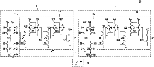
1. An integrated circuit comprising:
a first flip-flop configured to operate in synchronization with a clock signal, wherein the first flip-flop includes,
a multiplexer configured to receive a scan enabled signal, a scan input signal, a data input signal, and a reset input signal, the multiplexer configured to output an inverted signal of the scan input signal to a first node based on the scan enable signal, the multiplexer configured to output an inverted signal of the data input signal or a signal having a first level to the first node based on the reset input signal, the multiplexer configured to selectively output the inverted signal of the scan input signal, the inverted signal of the data input signal, or the signal having the first level to the first node based on the reset input signal and the scan enable signal,
a master latch configured to latch the output signal through the first node, and to output the latched signal, and
a slave latch configured to latch an output signal of the master latch and to output the latched output signal of the master latch.
|