| CPC H03K 19/018521 (2013.01) [H03K 3/356104 (2013.01)] | 15 Claims |

|
1. A level shifter, comprising:
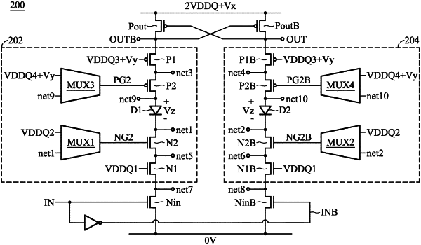
an input pair, having a first input transistor and a second input transistor which are controlled by an input signal and an inverse input signal of the level shifter, respectively;
a cross-coupled output pair, having a first output transistor and a second output transistor, wherein the second output transistor pulls up an output terminal of the level shifter to an overdrive voltage in response to a high-level state of the input signal, and the first output transistor pulls up an inverting output terminal of the level shifter to the overdrive voltage in response to a low-level state of the input signal;
a first protection circuit, coupled between the inverting output terminal and the first input transistor; and
a second protection circuit, coupled between the output terminal and the second input transistor;
wherein:
the overdrive voltage is twice a nominal voltage of the level shifter plus a delta voltage;
the first protection circuit comprises a first voltage-drop circuit that compensates for the delta voltage, and a first series of transistors, wherein the inverting output terminal is coupled to the first input transistor through the first voltage-drop circuit and the first series of transistors;
the second protection circuit comprises a second voltage-drop circuit that compensates for the delta voltage, and a second series of transistors, wherein the output terminal is coupled to the second input transistor through the second voltage-drop circuit and the second series of transistors;
the first protection circuit further comprises a third series of transistors coupled between the inverting output terminal and the first voltage-drop circuit;
the second protection circuit further comprises a fourth series of transistors coupled between the output terminal and the second voltage-drop circuit;
the first output transistor has a source terminal coupled to the overdrive voltage, a gate terminal coupled to the output terminal, and a drain terminal coupled to the inverting output terminal;
the second output transistor has a source terminal coupled to the overdrive voltage, a gate terminal coupled to the inverting output terminal, and a drain terminal coupled to the output terminal;
the third series of transistors comprises a fifth transistor and a sixth transistor;
the fifth transistor has a source terminal coupled to the drain terminal of the first output transistor, and a gate terminal biased by a third voltage;
the sixth transistor has a source terminal coupled to a drain terminal of the fifth transistor, and a drain terminal coupled to the first voltage-drop circuit;
in response to the low-level state of the input signal, a gate terminal of the sixth transistor is biased by a fourth voltage;
the fourth series of transistors comprises a seventh transistor and an eighth transistor;
the seventh transistor has a source terminal coupled to the drain terminal of the second output transistor, and a gate terminal biased by the third voltage;
the eighth transistor has a source terminal coupled to a drain terminal of the seventh transistor, and a drain terminal coupled to the second voltage-drop circuit;
in response to the high-level state of the input signal, a gate terminal of the eighth transistor is biased by the fourth voltage; and
the third voltage and the fourth voltage both are greater than the nominal voltage.
|