| CPC H03H 9/02125 (2013.01) [H03H 3/02 (2013.01); H03H 9/133 (2013.01); H03H 9/173 (2013.01); H03H 9/54 (2013.01); H03H 2003/021 (2013.01)] | 16 Claims |
|
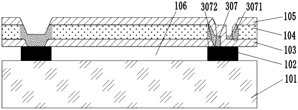
1. A thin film bulk acoustic wave resonator, comprising:
a bottom electrode layer, a piezoelectric layer, and a top electrode layer, which form a stack covering an acoustic reflection structure located at a surface of a substrate, wherein:
a portion of the piezoelectric layer and is depolarized to form a depolarized portion of which piezoelectricity is eliminated; and
along a direction perpendicular to the substrate, a projection of a part of the depolarized portion on the substrate is:
located outside of a projection of the acoustic reflection structure on the substrate,
located inside of a projection of the top electrode layer on the substrate, and
located inside of a projection of the bottom electrode layer on the substrate.
|