| CPC H02M 7/4818 (2021.05) [H02M 1/088 (2013.01); H02M 7/537 (2013.01)] | 18 Claims |

|
1. A semiconductor device comprising:
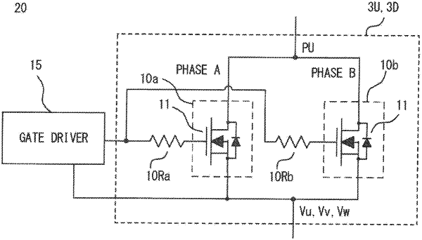
a first circuit including semiconductor switching elements connected in parallel, each semiconductor switching element having a first electrode, a second electrode, and a third electrode and being configured to be controlled, according to a voltage between the first electrode and the third electrode, to attain conduction or non-conduction between the second electrode and the third electrode; and
a controlling circuitry connected to the first electrode of each semiconductor switching element and configured to control the voltage between the first electrode and the third electrode, wherein
the semiconductor device is configured to satisfy a first condition that an impedance Zg on a first path between the first electrodes of the respective semiconductor switching elements is higher, by at least a set value, than an impedance Zs on a third path making connection between the third electrodes of the respective semiconductor switching elements,
the first condition is satisfied on the basis of an impedance at a resonance frequency of a series resonance circuit including: an inductance component on a second path making connection between the second electrodes of the respective semiconductor switching elements; an inductance component and a resistance component on the first path; and a capacitance component of each semiconductor switching element,
an inductive inductance element having a frequency characteristic that an impedance thereof increases at a resonance frequency of the series resonance circuit, is provided on the first path, and
the first condition is satisfied on the basis of the impedance at the resonance frequency of the series resonance circuit including the inductive inductance element.
|