| CPC H02H 9/041 (2013.01) [H01L 27/0262 (2013.01); H02H 9/046 (2013.01)] | 12 Claims |

|
1. An apparatus comprising:
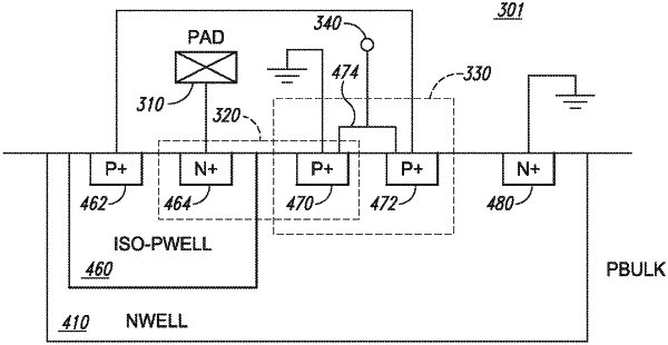
a bulk material doped with a first dopant type, wherein the bulk material includes a first well doped with a second dopant type, wherein the first well includes a first region, a second region, and a second well doped with the second dopant type, wherein the second well includes a third region doped with the first dopant type, wherein the third region, the second well, the first well, and the second region together form a thyristor, wherein the first region and the first well are coupled to a reference node, wherein the third region is coupled to a pad configured to provide an input signal; and
a gate formed on a surface of the bulk material overlapping an area between the first region and the second region, wherein the gate is coupled to a trigger voltage source configured to set the trigger voltage of the thyristor.
|