| CPC H01S 5/06246 (2013.01) [H01S 5/0261 (2013.01); H01S 5/042 (2013.01); H01S 5/062 (2013.01); H01S 5/0625 (2013.01); H01S 5/06258 (2013.01); H01S 5/06817 (2013.01); H01S 5/124 (2013.01); G02F 1/025 (2013.01); H01S 5/026 (2013.01); H01S 5/0265 (2013.01); H01S 5/12 (2013.01); H01S 2301/02 (2013.01)] | 15 Claims |
|
1. A method of operating an optoelectronic device comprising an optical waveguide section that includes a semiconductor core, the method comprising:
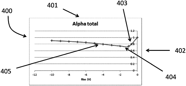
determining, based on Franz-Keldysh effect, Free carrier plasma effect, and Inter-valence band absorption, a range for a negative bias voltage for the optical waveguide section for which an optical loss of the semiconductor core is lower than an optical loss at zero bias for an operating wavelength range of the optoelectronic device;
selecting a bias voltage within the operating wavelength range; and
applying the bias voltage to the optical waveguide section.
|