| CPC H01S 5/04252 (2019.08) [G03B 21/2033 (2013.01); H01S 5/04253 (2019.08); H01S 5/04254 (2019.08); H01S 5/11 (2021.01); H01S 5/2054 (2013.01); H01S 5/341 (2013.01); B82Y 20/00 (2013.01); H01S 5/021 (2013.01); H01S 5/04257 (2019.08); H01S 5/185 (2021.01); H01S 5/4012 (2013.01); H01S 5/4093 (2013.01); H01S 5/42 (2013.01); H01S 2301/176 (2013.01)] | 6 Claims |

|
1. A light emitting device comprising:
a substrate;
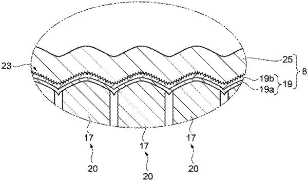
a laminated structure that is provided on the substrate and that includes a plurality of columnar portions; and
an electrode that is provided at an opposite side of the laminated structure from the substrate,
wherein the columnar portion includes a first semiconductor layer, a second semiconductor layer of a conductivity type different from that of the first semiconductor layer, and a light emitting layer located between the first semiconductor layer and the second semiconductor layer, and
the electrode is connected to the second semiconductor layers in the plurality of columnar portions, and includes:
a first electrode layer formed of a material that has a work function smaller than that of the second semiconductor layer, and
a second electrode layer that is connected to the first electrode layer and that has a work function smaller than that of the first electrode layer, and
an interface between the first electrode layer and the second electrode layer has an uneven shape that includes a plurality of peaks and valleys, and the peaks have a height of 10 nm or less.
|