|
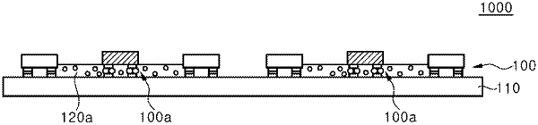
1. A display panel, comprising: a circuit board including first pads; first light emitting devices disposed on the circuit board and including pads; at least one second light emitting device disposed on the circuit board and including pads; metal bonding layers disposed between the pads of the first light emitting devices and the first pads on the circuit board; and a conductive material layer electrically connecting the pads of the second light emitting device to the first pads on the circuit board, wherein the conductive material layer includes a first region and a second region, wherein the first region of the conductive material layer is disposed between one of the pads of the second light emitting device and one of the first pads, and the second region of the conductive material layer extends from the first region and does not overlap the one of the pads of the second light emitting device, and wherein the at least one second light emitting device and at least one of the first light emitting device have a same thickness, and an upper surface of the at least one second light emitting device is placed higher than that of the at least one first light emitting device.
|