| CPC H01L 33/44 (2013.01) [H01L 33/46 (2013.01); H01L 33/007 (2013.01); H01L 33/20 (2013.01); H01L 33/36 (2013.01); H01L 2933/0016 (2013.01); H01L 2933/0025 (2013.01)] | 6 Claims |
|
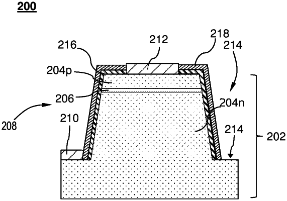
1. A light emitting diode (LED) device comprising:
a mesa comprising semiconductor layers, the semiconductor layers including an N-type layer, an active layer, and a P-type layer, the mesa having a top surface and at least one side wall, the at least one side wall defining a trench having a bottom surface;
a passivation layer on the at least one side wall and on the top surface of the mesa and not on the bottom surface of the trench, the passivation layer comprising a low-refractive index material, the low-refractive index material having a refractive index of about 1 and selected from the group consisting of, porous silicon nitride (SiN), porous titanium oxide (TiOx), porous aluminum oxide (AlOx), porous hafnium oxide (HfOx), porous niobium oxide (NbOx), porous aluminum indium gallium nitride (AlInGaN), and porous aluminum indium gallium phosphide (AlInGaP);
an electrical passivation layer between the passivation layer and the mesa, the electrical passivation layer comprising one or more of silicon nitride (SiN), titanium oxide (TiO2), niobium oxide (NbO2), aluminum oxide (Al2O3), hafnium oxide (HfO2), aluminum nitride (AlN), silicon dioxide (SiO2), and hafnium-doped silicon dioxide (HfSiO2);
a p-type contact on the top surface of the mesa; and
an n-type contact on the bottom surface of the trench.
|