US 11,901,487 B2
Ultrathin solid state dies and methods of manufacturing the same
Vladimir Odnoblyudov, Eagle, ID (US); and Martin F. Schubert, Mountain View, CA (US)
Assigned to Micron Technology, Inc., Boise, ID (US)
Filed by Micron Technology, Inc., Boise, ID (US)
Filed on Oct. 10, 2022, as Appl. No. 18/045,331.
Application 15/474,786 is a division of application No. 13/918,745, filed on Jun. 14, 2013, granted, now 9,653,647.
Application 18/045,331 is a continuation of application No. 17/099,276, filed on Nov. 16, 2020, granted, now 11,469,350.
Application 17/099,276 is a continuation of application No. 16/804,504, filed on Feb. 28, 2020, granted, now 10,840,410.
Application 16/804,504 is a continuation of application No. 16/377,897, filed on Apr. 8, 2019, granted, now 10,580,935.
Application 16/377,897 is a continuation of application No. 16/022,409, filed on Jun. 28, 2018, granted, now 10,256,367.
Application 16/022,409 is a continuation of application No. 15/474,786, filed on Mar. 30, 2017, granted, now 10,103,290.
Prior Publication US 2023/0109959 A1, Apr. 13, 2023
Int. Cl. H01L 21/00 (2006.01); H01L 33/20 (2010.01); H01L 33/08 (2010.01); H01L 21/02 (2006.01); H01L 33/38 (2010.01); H01L 33/00 (2010.01); H01L 33/12 (2010.01); H01L 33/48 (2010.01); H01L 33/62 (2010.01)
CPC H01L 33/20 (2013.01) [H01L 21/02104 (2013.01); H01L 33/0075 (2013.01); H01L 33/0093 (2020.05); H01L 33/08 (2013.01); H01L 33/12 (2013.01); H01L 33/38 (2013.01); H01L 33/483 (2013.01); H01L 33/62 (2013.01); H01L 2933/0016 (2013.01)] 20 Claims
OG exemplary drawing
 
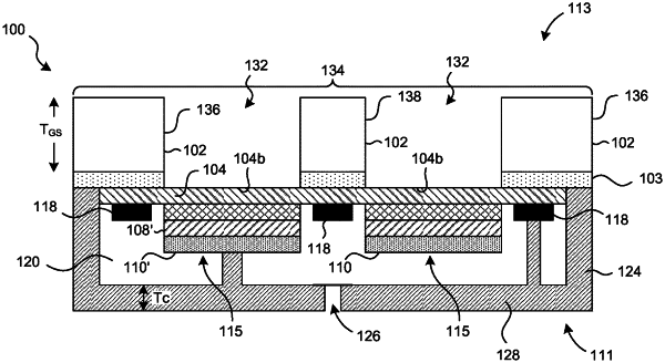
1. A solid state transducer (SST) die, comprising:
a growth substrate;
a continuous layer of a first semiconductor material coupled to the growth substrate;
a plurality of SST structures on the growth substrate, each SST structure including:
a portion of the continuous layer of the first semiconductor material,
a second semiconductor material, and
a light emitting material between the portion of the continuous layer of the first semiconductor material and the second semiconductor material;
a first contact in contact with the continuous layer of the first semiconductor material; and
a second contact in contact with the second semiconductor material of each of the plurality of SST structures,
wherein the growth substrate includes a plurality of openings, each opening aligned with the light emitting material of a corresponding one of the plurality of SST structures.