| CPC H01L 33/20 (2013.01) [H01L 24/81 (2013.01); H01L 33/005 (2013.01); H01L 24/14 (2013.01); H01L 2933/0066 (2013.01)] | 20 Claims |
|
1. A method for transferring a chip, comprising:
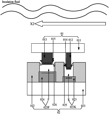
disposing a target substrate in a sealed chamber, wherein the target substrate comprises a first alignment bonding structure and a second alignment bonding structure, and the chip comprises a first chip bonding structure and a second chip bonding structure;
applying a charge of a first polarity to the first alignment bonding structure, applying a charge of a second polarity to the first chip bonding structure, and injecting an insulation fluid flowing in a first direction into the sealed chamber, such that the first chip bonding structure is aligned with the first alignment bonding structure, wherein the first polarity is different from the second polarity;
applying the charge of the first polarity to the first alignment bonding structure, the first chip bonding structure and the second chip bonding structure respectively, applying the charge of the second polarity to the second alignment bonding structure, and changing the insulation fluid to flow in a second direction, such that the second chip bonding structure is aligned with the second alignment bonding structure, wherein the second direction is different from the first direction; and
applying a bonding force to the chip, such that the first chip bonding structure is bonded to the first alignment bonding structure and the second chip bonding structure is bonded to the second alignment bonding structure.
|