| CPC H01L 33/02 (2013.01) [H01L 22/12 (2013.01); H01L 22/14 (2013.01); H01L 24/24 (2013.01); H01L 25/0753 (2013.01); H01L 33/62 (2013.01); H01L 33/36 (2013.01); H01L 2924/0002 (2013.01); H01L 2933/0033 (2013.01); H01L 2933/0066 (2013.01)] | 14 Claims |
|
1. A method of manufacturing a light-emitting device, comprising:
providing a growth substrate;
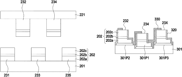
forming a first plurality of blocks of semiconductor stack and a second plurality of blocks of semiconductor stack on the growth substrate, wherein the first plurality of blocks of semiconductor stack comprises a first block of semiconductor stack, the second plurality of blocks of semiconductor stack comprises a second block of semiconductor stack, and the first block of semiconductor stack and the second block of semiconductor stack are not adjacent to each other;
providing a substrate comprising a first surface and a second surface; and
bonding the first block of semiconductor stack and the second block of semiconductor stack to the substrate in a configuration that the first block of semiconductor stack and the second block of semiconductor stack are located adjacent to each other,
wherein the first block of semiconductor stack and the second block of semiconductor stack are configured to emit same color lights,
wherein a difference between a first dominant wavelength of the first block of semiconductor stack and a second dominant wavelength of the second block of semiconductor stack is greater than or equal to 1 nm, and
wherein the first block of semiconductor stack comprises a first average dominant wavelength, the second block of semiconductor stack comprises a second average dominant wavelength, and a difference between the first average dominant wavelength and the second average dominant wavelength is larger than the difference of a first dominant wavelength of the first block of semiconductor stack and a second dominant wavelength of the second block of semiconductor stack.
|