| CPC H01L 31/022466 (2013.01) [H01L 31/095 (2013.01); H01L 31/102 (2013.01); H01L 31/1884 (2013.01); H01L 31/202 (2013.01)] | 20 Claims |
|
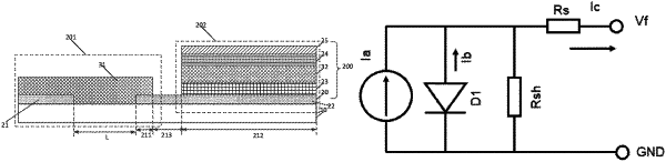
1. A photodiode, comprising:
a substrate;
a first electrode disposed on the substrate and comprising a first sub-part and a second sub-part disposed at an interval, wherein the second sub-part comprises a first end and a second end;
a connecting part disposed on the first sub-part, the first end, and the substrate corresponding to a gap between the first sub-part and the second sub-part, wherein the connecting part connects the first sub-part with the first end to form a series resistance part;
an electron transport layer disposed on the second end;
a light converting part disposed on the electron transport layer;
a hole transport layer disposed on the light converting part; and
a second electrode disposed on the hole transport layer.
|