| CPC H01L 29/94 (2013.01) [H01L 29/66189 (2013.01); H01L 21/266 (2013.01); H01L 21/26513 (2013.01); H01L 21/26586 (2013.01); H01L 29/401 (2013.01)] | 37 Claims |
|
1. An integrated circuit comprising:
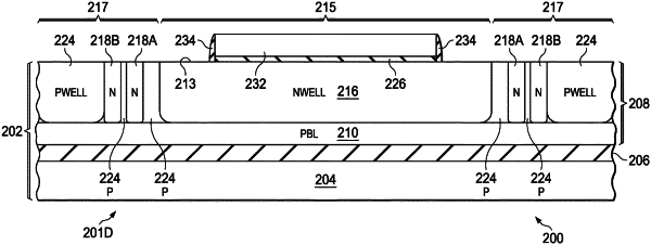
a semiconductor-on-insulator (SOI) substrate having a semiconductor layer over a buried insulator layer, the semiconductor layer including white space regions that include a P-type well (PWELL) region;
an electronic device that includes an N-type well (NWELL) region formed in the semiconductor layer, a dielectric formed over the NWELL region, and a polysilicon plate over the dielectric; and
a sacrificial NWELL ring adjacent to and separated from the NWELL region by a first gap.
|