| CPC H01L 29/7853 (2013.01) [H01L 27/0886 (2013.01); H01L 29/0847 (2013.01); H01L 29/66795 (2013.01)] | 23 Claims |

|
1. An integrated circuit structure, comprising:
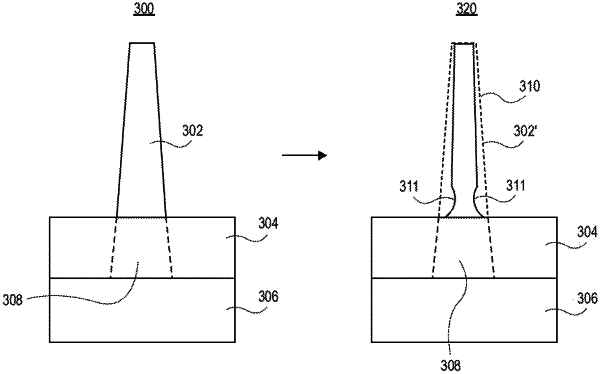
a semiconductor fin having a protruding fin portion above an isolation structure above a substrate, the protruding fin portion having substantially vertical upper sidewalls and outwardly tapered lower sidewalls, and the semiconductor fin further comprising a sub-fin portion on the substrate and within an opening in the isolation structure, the sub-fin portion in contact with the protruding portion, and the sub-fin portion having an upper horizontal surface extending laterally beyond the protruding fin portion;
a gate stack over and conformal with the protruding fin portion of the semiconductor fin;
a first source or drain region at a first side of the gate stack; and
a second source or drain region at a second side of the gate stack opposite the first side of the gate stack.
|