| CPC H01L 29/7851 (2013.01) [H01L 21/266 (2013.01); H01L 21/31155 (2013.01); H01L 21/764 (2013.01); H01L 21/7682 (2013.01); H01L 21/76825 (2013.01); H01L 21/76831 (2013.01); H01L 21/76897 (2013.01); H01L 21/823821 (2013.01); H01L 21/823828 (2013.01); H01L 21/823864 (2013.01); H01L 21/823871 (2013.01); H01L 29/0847 (2013.01); H01L 29/41725 (2013.01); H01L 29/41766 (2013.01); H01L 29/41791 (2013.01); H01L 29/4991 (2013.01); H01L 29/6653 (2013.01); H01L 29/66545 (2013.01); H01L 29/66795 (2013.01); H01L 29/785 (2013.01); H01L 21/28518 (2013.01); H01L 21/76224 (2013.01); H01L 21/76843 (2013.01); H01L 21/76855 (2013.01); H01L 2221/1063 (2013.01)] | 20 Claims |

|
1. A method comprising:
forming a gate stack over a semiconductor fin;
forming an epitaxial source/drain region in the semiconductor fin adjacent the gate stack;
depositing a first dielectric layer over the gate stack and over the epitaxial source/drain region;
forming an opening in the first dielectric layer to expose the epitaxial source/drain region;
depositing a sacrificial material within the opening;
depositing a conductive material over the sacrificial material within the opening;
removing the sacrificial material to form a recess; and
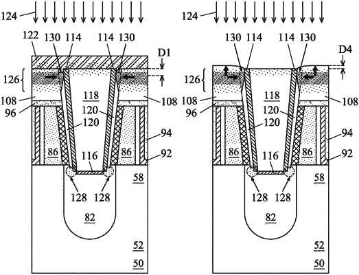
implanting the first dielectric layer with a dopant, wherein after implanting the first dielectric layer the recess is covered by the first dielectric layer.
|
|
9. A method comprising:
forming a fin protruding from a semiconductor substrate;
forming a gate structure over a channel region of the fin;
forming an epitaxial source/drain region in the fin adjacent the channel region;
forming a first inter-layer dielectric (ILD) layer over the epitaxial source/drain region;
forming a second ILD layer over the gate structure and over the first ILD;
forming a source/drain contact penetrating through the first ILD and the second ILD to physically contact the epitaxial source/drain region, wherein the source/drain contact is surrounded by a first spacer layer and a second spacer layer;
etching the first spacer layer to expose sidewalls of the second spacer layer; and
performing an implantation process on the second ILD, wherein the implantation process laterally expands a first portion of the second ILD to physically contact an exposed sidewall of the second spacer layer.
|
|
16. A method comprising:
forming an epitaxial source/drain region in a semiconductor fin;
forming an isolation region over the epitaxial source/drain region;
forming a contact on the epitaxial source/drain region, wherein an air gap separates the contact and the isolation region; and
sealing the air gap, comprising implanting the isolation region with a dopant.
|