| CPC H01L 29/7848 (2013.01) [H01L 21/02532 (2013.01); H01L 21/76224 (2013.01); H01L 21/823418 (2013.01); H01L 21/823431 (2013.01); H01L 21/823437 (2013.01); H01L 21/823481 (2013.01); H01L 27/0886 (2013.01); H01L 29/0649 (2013.01); H01L 29/165 (2013.01); H01L 29/66545 (2013.01); H01L 29/66636 (2013.01); H01L 29/66795 (2013.01); H01L 29/785 (2013.01); H01L 2029/7858 (2013.01)] | 20 Claims |
|
1. A device comprising:
a semiconductor fin structure disposed over a substrate;
a dielectric isolation structure disposed on the substrate;
a gate structure disposed over a first portion of the semiconductor fin structure; and
a source/drain feature disposed over a second portion of the semiconductor fin structure, the source/drain feature including:
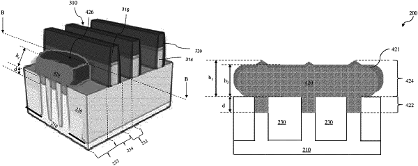
a first lower portion and a second lower portion that are isolated from each other by the dielectric isolation structure; and
a single upper portion disposed over the first and second lower portions, wherein the single upper portion is merged from the first and second lower portions, wherein the single upper portion has a top surface facing away from a top surface of the substrate, wherein the top surface of the single upper portion includes a first multi-facet surface and a flat surface interfacing with the first multi-facet surface, the first multi-facet surface being positioned at a higher level above the substrate than the flat surface and the flat surface being parallel to a top surface of the substrate, wherein the single upper portion further includes a bottom surface that opposes the flat surface of the top surface of the single upper portion, the bottom surface of the single upper portion facing the substrate and interfacing with a top surface of the dielectric isolation structure, the top surface of the dielectric isolation structure facing away from the substrate, and
wherein the first lower portion interfaces with a first portion of the semiconductor fin structure, the first portion of the semiconductor fin structure extending to a first height above the substrate,
wherein the dielectric isolation structure interfaces with the first portion of the semiconductor fin structure and extends to a second height over the substrate, the second height being different than the first height, and
wherein the single upper portion and the first and second lower portions are formed of the same material, wherein the material includes a material selected from the group consisting of SiGe and SiC.
|