| CPC H01L 29/78391 (2014.09) [H01L 21/0234 (2013.01); H01L 21/02181 (2013.01); H01L 21/02356 (2013.01); H01L 29/40111 (2019.08); H01L 29/516 (2013.01); H01L 29/6684 (2013.01); H01L 29/66795 (2013.01); H01L 29/7851 (2013.01)] | 20 Claims |
|
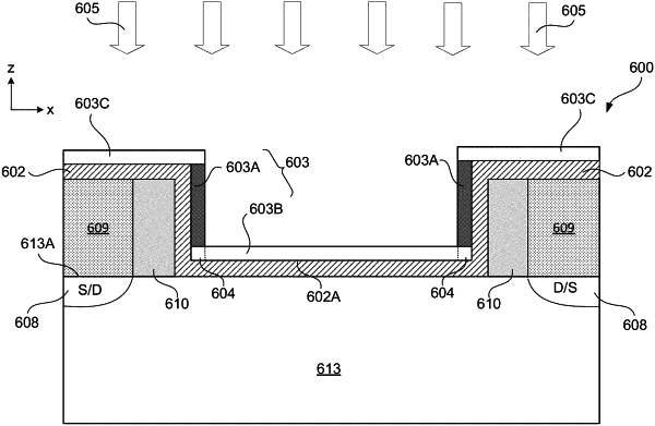
1. A method, comprising:
forming a pair of opposing spacers on a fin;
depositing an amorphous dielectric layer in an opening between the pair of opposing spacers, comprising:
depositing a first portion of the amorphous dielectric layer on the fin; and
depositing a second portion of the amorphous dielectric layer on sidewalls of the pair of opposing spacers; and
performing a plasma treatment on the amorphous dielectric layer, wherein the plasma treatment converts the first portion of the amorphous dielectric layer into a crystalline dielectric layer without converting the second portion of the amorphous dielectric layer.
|