| CPC H01L 29/7786 (2013.01) [H01L 29/401 (2013.01); H01L 29/41775 (2013.01); H01L 29/42316 (2013.01); H01L 29/66462 (2013.01)] | 20 Claims |
|
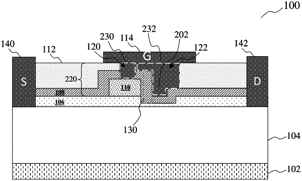
1. A transistor comprising:
a buffer layer;
source and drain contacts on the buffer layer,
a barrier layer on the buffer layer, wherein the barrier layer is arranged between the source and drain contacts;
a conductive member on the barrier layer, wherein the conductive member comprises a p-doped III-V compound;
a dielectric stack on the barrier layer and on the conductive member, wherein the dielectric stack comprises a first dielectric layer and a second dielectric layer on the first dielectric layer,
a first trench entirely through the first dielectric layer and the second dielectric layer such that a top surface of the conductive member, at least one sidewall of the first dielectric layer and at least one sidewall of the second dielectric layer are exposed in the first trench, wherein the first dielectric layer contacts the top surface the conductive member;
a second trench entirely through the second dielectric layer such that a top surface of the first dielectric layer and at least one sidewall of the second dielectric layer are exposed in the second trench; and
a gate metal on the dielectric stack, wherein the gate metal contacts the conductive member through the first trench, and wherein the gate metal contacts the first dielectric layer through the second trench.
|