| CPC H01L 29/66818 (2013.01) [H01L 21/0262 (2013.01); H01L 21/02532 (2013.01); H01L 21/02661 (2013.01); H01L 21/823807 (2013.01); H01L 21/823821 (2013.01); H01L 27/0924 (2013.01); H01L 29/1037 (2013.01); H01L 29/161 (2013.01); H01L 29/6681 (2013.01); H01L 29/7851 (2013.01)] | 20 Claims |
|
1. A semiconductor device comprising:
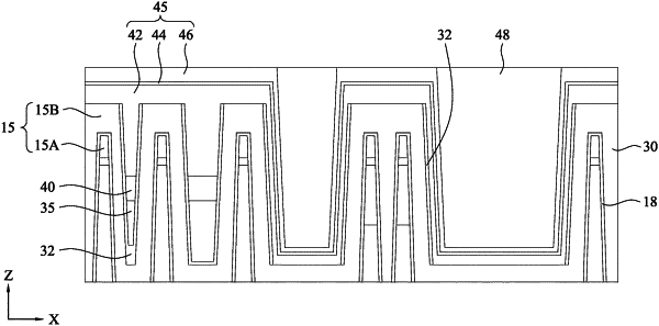
a semiconductor fin disposed over a semiconductor substrate and extending in a first direction, the semiconductor fin including a channel region and a bottom region on which the channel region is disposed;
a liner dielectric layer disposed on side walls of the bottom region;
an isolation insulating layer from which the channel region protrudes and in which the bottom region is embedded; and
a gate structure disposed over the channel region of the semiconductor fin and extending in a second direction crossing the first direction, wherein:
a cap semiconductor layer is disposed on the channel region,
a top of the liner dielectric layer is only partially covered by the cap semiconductor layer, and
a thickness of the cap semiconductor layer on the liner dielectric layer is greater than a thickness of the cap semiconductor layer at a 50% height of the channel region.
|