| CPC H01L 29/6681 (2013.01) [H01L 21/823431 (2013.01); H01L 21/823468 (2013.01); H01L 29/7851 (2013.01)] | 20 Claims |
|
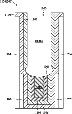
1. A method, comprising:
forming a gate trench over a semiconductor fin, the gate trench including a top portion over a bottom portion that is narrower than the top portion;
depositing a glue layer in the gate trench, the glue layer including a second sub-layer over a first sub-layer, wherein the first and the second sub-layers differ in composition, and wherein a portion of the first sub-layer completely fills the bottom portion of the gate trench; and
removing a portion of the glue layer from the top portion of the gate trench to expose the portion of the first sub-layer in the bottom portion of the gate trench.
|