| CPC H01L 29/66795 (2013.01) [H01L 21/823418 (2013.01); H01L 21/823431 (2013.01); H01L 23/481 (2013.01); H01L 29/0847 (2013.01); H01L 29/7851 (2013.01)] | 20 Claims |

|
1. A semiconductor device comprising:
a functional gate structure including a first source/drain region located a first end of a semiconductor channel material structure and a second source/drain region located at a second end of the semiconductor channel material structure; and
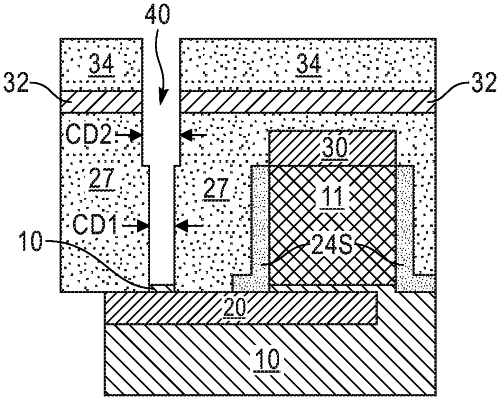
a contact rail located laterally adjacent to the functional gate structure and contacting a surface of the first source/drain region of the functional gate structure, wherein the contact rail has a lower portion having a first critical dimension and an upper portion having a second critical dimension that is greater than the first critical dimension, wherein the first critical dimension is 25 nm or less.
|