| CPC H01L 29/6656 (2013.01) [H01L 21/823431 (2013.01); H01L 21/823821 (2013.01); H01L 27/0886 (2013.01); H01L 29/42392 (2013.01); H01L 29/6653 (2013.01); H01L 29/66553 (2013.01); H01L 29/78696 (2013.01); H01L 21/823468 (2013.01)] | 20 Claims |
|
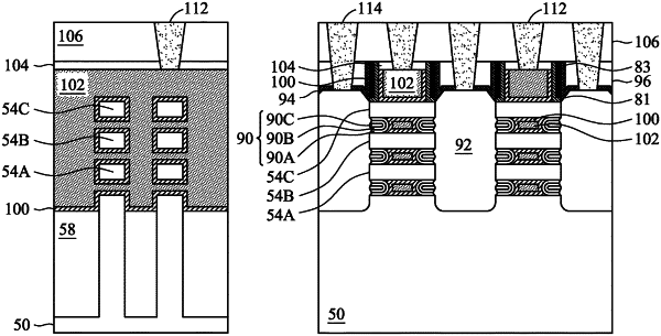
8. A semiconductor device comprising:
a semiconductor substrate;
a channel region on the semiconductor substrate;
a gate structure on the channel region;
a source/drain region adjacent the gate structure; and
an inner spacer adjacent the channel region, wherein the inner spacer is between the source/drain region and the gate structure, wherein the inner spacer comprises:
a first inner spacer layer contacting the gate structure and the source/drain region;
a second inner spacer layer contacting the first inner spacer layer and the source/drain region; and
a third inner spacer layer contacting the second inner spacer layer and the source/drain region, wherein a first sidewall of the inner spacer adjacent the source/drain region is W-shaped in a cross-sectional view, wherein a second sidewall of the inner spacer adjacent the gate structure is U-shaped in the cross-sectional view, wherein the first inner spacer layer, the second inner spacer layer, and the third inner spacer layer comprise carbon, and wherein a first atomic percentage of carbon in the first inner spacer layer is greater than a second atomic percentage of carbon in the second inner spacer layer and a third atomic percentage of carbon in the third inner spacer layer.
|