| CPC H01L 29/6656 (2013.01) [B82Y 10/00 (2013.01); H01L 21/02164 (2013.01); H01L 21/02236 (2013.01); H01L 21/31116 (2013.01); H01L 23/291 (2013.01); H01L 23/3171 (2013.01); H01L 29/0653 (2013.01); H01L 29/0673 (2013.01); H01L 29/401 (2013.01); H01L 29/42392 (2013.01); H01L 29/6681 (2013.01); H01L 29/66553 (2013.01); H01L 29/775 (2013.01); H01L 29/7853 (2013.01); H01L 29/78696 (2013.01)] | 20 Claims |
|
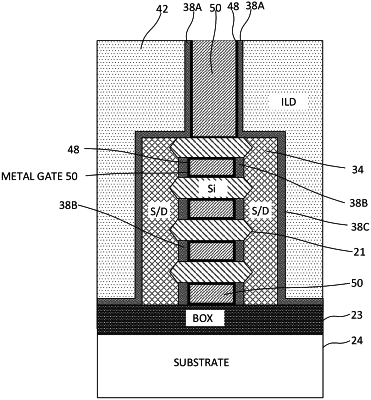
1. A semiconductor nanosheet device comprising:
epitaxial source-drain regions on opposite sides of a gate stack;
a vertical stack of nanosheets each extending in a horizontal direction between the epitaxial source-drain regions, and each comprising end portions in contact with the epitaxial source-drain regions and a center portion that extends between the end portions;
the gate stack surrounding each of the center portions; and
pairs of inner spacers on opposite sides of the gate stack, each pair separating a portion of the gate stack from the epitaxial source-drain regions, wherein:
a middle portion of each nanosheet is wider in the horizontal direction than a top portion and a bottom portion of the respective nanosheet.
|