| CPC H01L 29/66545 (2013.01) [H01L 27/127 (2013.01); H01L 27/1288 (2013.01); H01L 29/401 (2013.01); H01L 29/42392 (2013.01)] | 20 Claims |
|
1. A method comprising,
forming a first fin and a second fin over a substrate, the first and second fins each comprising alternately stacking first semiconductor layers and second semiconductor layers;
forming dummy gate structures over the first and second fins, and gate spacers on either side of the dummy gate structures;
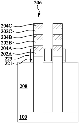
removing the dummy gate structures to form a first gate trench over the first fin and a second gate trench over the second fin;
removing the first semiconductor layers such that the second semiconductor layers are suspended in the first and second gate trenches;
depositing a first gate dielectric layer around each of the second semiconductor layers and a second gate dielectric layer around the first gate dielectric layer;
performing an atomic layer deposition (ALD) process to form a hard mask layer around the second gate dielectric layer, the ALD process comprising pulsing a first precursor into a deposition chamber for a first pulse time longer than a time within a range of 0.8 seconds to 1.2 seconds;
patterning the hard mask layer; and
with the patterned hard mask layer in place, etching a portion of the second gate dielectric layer in the second gate trench.
|