| CPC H01L 29/66462 (2013.01) [H01L 29/452 (2013.01); H01L 29/7786 (2013.01); H01L 29/1066 (2013.01); H01L 29/402 (2013.01); H01L 29/41758 (2013.01)] | 20 Claims |

|
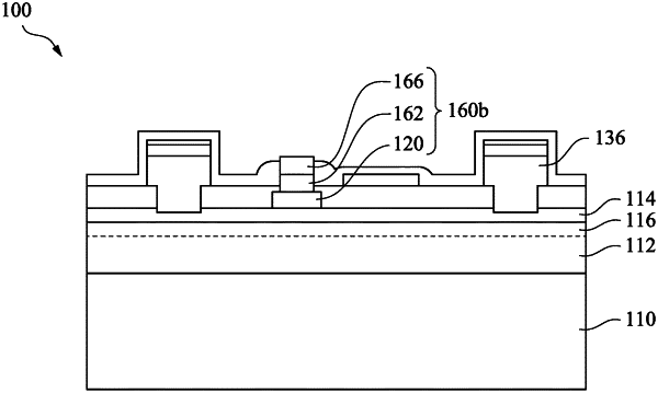
1. A device, comprising:
a first III-V compound layer;
a second III-V compound layer over the first III-V compound layer;
a dielectric layer over the second III-V compound layer;
a source/drain contact extending through the dielectric layer to the second III-V compound layer, wherein the source/drain contact is in contact with a top surface of the dielectric layer and an inner sidewall of the dielectric layer;
a metal-containing layer over and in contact with the source/drain contact and a portion of the metal-containing layer is directly above the dielectric layer; and
a metal contact over and in contact with the metal-containing layer, wherein a bottommost surface of the metal-containing layer is wider than a bottommost surface of the metal contact and a pate field plate between a pate structure and the source/drain contact.
|