| CPC H01L 29/41791 (2013.01) [H01L 21/764 (2013.01); H01L 21/7682 (2013.01); H01L 21/76232 (2013.01); H01L 21/76843 (2013.01); H01L 21/823821 (2013.01); H01L 21/823871 (2013.01); H01L 21/823878 (2013.01); H01L 23/5226 (2013.01); H01L 29/401 (2013.01)] | 20 Claims |

|
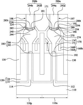
1. A device comprising:
an active region;
a gate structure across the active region and extending in a first direction;
a source/drain epitaxial structure over the active region and adjacent the gate structure;
an epitaxial layer over the source/drain epitaxial structure, wherein a maximal width of the epitaxial layer is less than a maximal width of the source/drain epitaxial structure in the first direction;
a metal alloy layer over the epitaxial layer;
a contact over the metal alloy layer; and
a contact etch stop layer lining sidewalls of the source/drain epitaxial structure, wherein the metal alloy layer is spaced apart from the contact etch stop layer.
|