| CPC H01L 29/41775 (2013.01) [H01L 21/823475 (2013.01); H01L 27/0886 (2013.01); H01L 27/0924 (2013.01); H01L 27/1211 (2013.01); H01L 29/0649 (2013.01); H01L 29/41791 (2013.01); H01L 29/66795 (2013.01); H01L 29/785 (2013.01); H10B 10/12 (2023.02); H01L 21/823425 (2013.01); H01L 27/0207 (2013.01)] | 17 Claims |
|
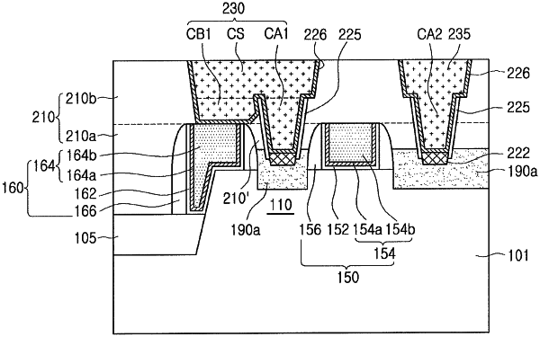
1. A semiconductor device, comprising:
a substrate;
a fin-type active pattern extended on the substrate in a first direction;
a gate structure extended on the substrate in a second direction different from the first direction, the gate structure intersecting the fin-type active pattern, and the gate structure including sidewall spacers on opposite sidewalls thereof;
an active area on a side of the gate structure in the fin-type active pattern and serving as a source/drain region;
an insulating layer on the substrate, the insulating layer covering the fin-type active pattern and the gate structure;
a shared contact plug penetrating through the insulating layer, the shared contact plug including:
a first lower portion and a second lower portion connected to the active area and the gate structure, respectively, the insulating layer having a first portion between the first lower portion and the second lower portion, and
an upper portion connecting upper surfaces of the first lower portion and the second lower portion; and
a silicon nitride film between the first lower portion and the second lower portion, the silicon nitride film surrounding a sidewall of the first lower portion and the second lower portion,
wherein the insulating layer includes a second portion between the silicon nitride film and a corresponding one of the sidewall spacers of the gate structure, and
wherein a bottom of the second lower portion has a flat area and is at a level higher than a bottom of the first lower portion.
|