| CPC H01L 29/2003 (2013.01) [H01L 21/0254 (2013.01); H01L 21/02378 (2013.01); H01L 21/02488 (2013.01); H01L 21/02527 (2013.01); H01L 21/76871 (2013.01); H01L 21/76897 (2013.01); H01L 24/94 (2013.01); H01L 29/1602 (2013.01); H01L 29/205 (2013.01); H01L 29/267 (2013.01); H01L 29/66462 (2013.01)] | 11 Claims |
|
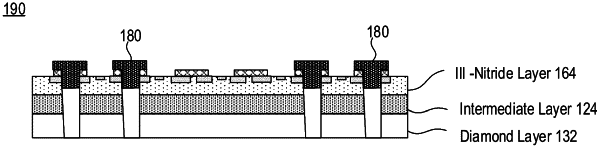
1. A method for processing a semiconductor wafer, comprising:
disposing and patterning a first metal layer on a semiconductor layer of a semiconductor wafer, wherein the semiconductor wafer includes a substrate wafer, a bonding layer, a diamond layer, an intermediate layer and the semiconductor layer;
drilling one or more holes from the first metal layer toward the substrate wafer to thereby form one or more vias that extend from the first metal layer into the substrate wafer;
disposing a second metal layer on the first metal layer and in a portion of the one or more vias; and
removing the substrate wafer and the bonding layer to expose a surface of the diamond layer.
|