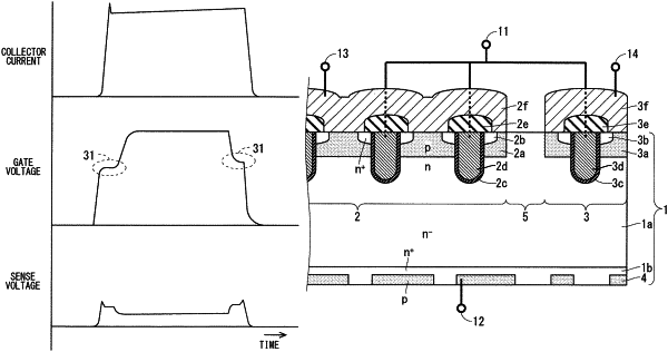
| CPC H01L 29/1095 (2013.01) [H01L 29/32 (2013.01); H01L 29/7397 (2013.01)] | 5 Claims |

|
1. A semiconductor device, comprising:
a semiconductor substrate of first conductivity type;
a first IGBT portion selectively disposed on a first main surface of the semiconductor substrate;
a second IGBT portion disposed on the first main surface of the semiconductor substrate, spaced from the first IGBT portion, and used for detection of a current passing through the first IGBT portion; and
an impurity region of second conductivity type selectively disposed on a second main surface opposite to the first main surface of the semiconductor substrate, wherein
an area ratio of the impurity region within a second range to an area of the second range is lower than an area ratio of the impurity region within a first range to an area of the first range, the second range corresponding to the second IGBT portion on the second main surface, the first range corresponding to the first IGBT portion on the second main surface.
|