| CPC H01L 29/0673 (2013.01) [H01L 21/823418 (2013.01); H01L 21/823431 (2013.01); H01L 29/0649 (2013.01); H01L 29/0843 (2013.01); H01L 29/66553 (2013.01); H01L 29/66795 (2013.01); H01L 29/7851 (2013.01)] | 20 Claims |
|
1. A method comprising:
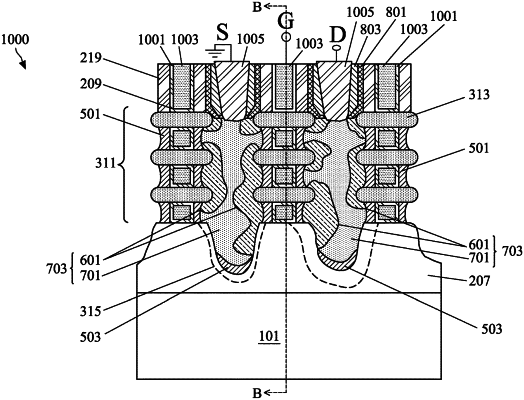
forming an opening through a multilayer stack and into a substrate;
depositing a first semiconductor material, the first semiconductor material comprising a first percentage volume of germanium;
depositing a second semiconductor material adjacent to the first semiconductor material, the second semiconductor material being deposited below a bottommost surface of the first semiconductor material, the second semiconductor material comprising a second percentage volume of germanium that is greater than the first percentage volume of germanium;
removing sacrificial layers of the multilayer stack, the second semiconductor material being electrically coupled to a stack of nanostructures;
prior to the depositing the first semiconductor material, depositing a dielectric material in the opening;
forming an inner spacer between a first nanostructure and a second nanostructure of the stack of nanostructures from the dielectric material; and
after the depositing the first semiconductor material, removing excess dielectric material at the bottom of the opening using the first semiconductor material to protect the inner spacer.
|