| CPC H01L 29/0649 (2013.01) [H01L 21/823481 (2013.01); H01L 29/0843 (2013.01); H01L 29/66795 (2013.01); H01L 29/7851 (2013.01)] | 17 Claims |
|
1. A semiconductor device, comprising:
a substrate;
a gate structure disposed on the substrate;
a conductive layer disposed on the gate structure and electrically connected to the gate structure; and
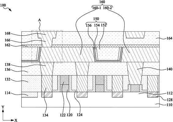
a dielectric structure disposed on the gate structure, wherein the dielectric structure comprises a first dielectric layer and an air gap spaced apart from the conductive layer by the first dielectric layer, and the first dielectric layer has a lateral surface defining a recess tapered toward the substrate, and the lateral surface of the first dielectric layer is exposed to the air gap.
|