| CPC H01L 29/0649 (2013.01) [H01L 21/764 (2013.01); H01L 21/7682 (2013.01); H01L 21/76841 (2013.01); H01L 21/76897 (2013.01); H01L 21/823864 (2013.01); H01L 21/823871 (2013.01); H01L 23/10 (2013.01); H01L 29/6656 (2013.01); H01L 29/6681 (2013.01); H01L 29/66545 (2013.01)] | 20 Claims |

|
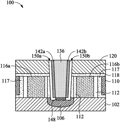
1. A device comprising:
a source/drain feature disposed on a substrate;
a gate stack disposed on the substrate and associated with the source/drain feature, the gate stack extending to a first height above the substrate;
a first interlayer dielectric layer disposed over the substrate;
a contact feature extending through the first interlayer dielectric layer to the source/drain feature;
an air gap disposed between the gate stack and the contact feature, the air gap extending from the source/drain feature to a second height above the substrate that is greater than the first height of the gate stack, the source/drain feature being exposed to the air gap;
a nitride layer disposed directly on and extending along a sidewall of the contact feature, the nitride layer exposed to the air gap; and
a seal layer disposed directly on the first interlayer dielectric layer, the nitride layer and the contact feature, the seal layer sealing the air gap such that the seal layer is exposed to the air gap.
|