| CPC H01L 28/87 (2013.01) [H10B 12/033 (2023.02); H10B 12/31 (2023.02)] | 17 Claims |
|
1. A method for forming a semiconductor device, the method comprising:
forming a transistor, wherein the transistor includes a channel along a first direction;
forming a pole placed in a second direction orthogonal to the first direction;
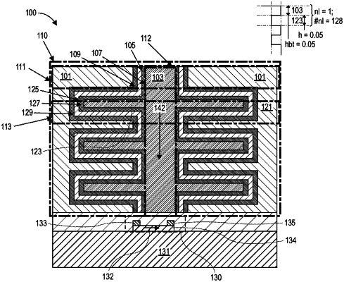
forming a first electrode surrounding and coupled to the pole;
forming a dielectric layer surrounding the first electrode, and
forming a second electrode surrounding the dielectric layer, wherein the first electrode, the dielectric layer, and the second electrode form a capacitor unit around the pole, wherein the capacitor unit is a first capacitor unit, and the method further comprises:
forming a second capacitor unit above the first capacitor unit, wherein forming the second capacitor unit includes:
forming a first electrode of the second capacitor unit surrounding and coupled to the pole and above the first capacitor unit;
forming a dielectric layer of the second capacitor unit surrounding the first electrode of the second capacitor, and
forming a second electrode of the second capacitor unit surrounding the dielectric layer of the second capacitor.
|