| CPC H01L 28/60 (2013.01) [H01G 4/38 (2013.01); H01L 23/49838 (2013.01); H01L 23/5227 (2013.01); H01L 23/66 (2013.01); H01L 24/06 (2013.01); H01L 28/90 (2013.01); H01L 2224/023 (2013.01)] | 19 Claims |

|
1. A semiconductor device comprising:
a semiconductor substrate;
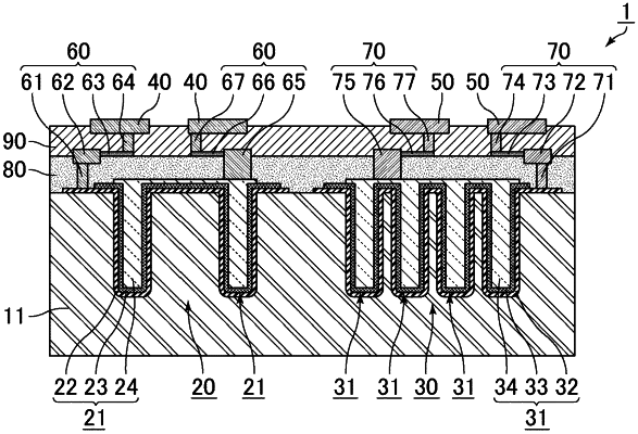
a first capacitance section on the semiconductor substrate, the first capacitance section including a first electrode layer, a first dielectric layer, and a second electrode layer;
a second capacitance section on the semiconductor substrate, the second capacitance section including a third electrode layer, a second dielectric layer, and a fourth electrode layer;
a first external electrode;
a second external electrode;
a third external electrode;
a fourth external electrode;
a first lead wire connecting the first external electrode to the first electrode layer;
a second lead wire connecting the second external electrode to the second electrode layer;
a third lead wire connecting the third external electrode to the third electrode layer; and
a fourth lead wire connecting the fourth external electrode to the fourth electrode layer, wherein
an inductance L1 is a sum of an inductance of the first and second lead wires,
an inductance L2 is a sum of an inductance of the third and fourth lead wires,
the first electrode layer and the second electrode layer of the first capacitance section are not connected to the third or fourth external electrodes,
the third electrode layer and the fourth electrode layer of the second capacitance section are not connected to the first or second external electrodes,
an electrostatic capacity C1 of the first capacitance section and an electrostatic capacity C2 of the second capacitance section are different, and
L1/L2=0.8 to 1.2 such that, when capacitance is changed between C1 and C2, impedance characteristics of the first capacitance section and the second capacitance section are equal in a high frequency range thereof where inductance is dominant with respect to impedance.
|