| CPC H01L 28/56 (2013.01) [H01G 4/012 (2013.01); H01G 4/30 (2013.01); H01L 23/5226 (2013.01); H10B 51/00 (2023.02)] | 19 Claims |
|
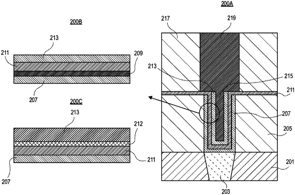
1. A capacitor, comprising:
a first metal layer in a trench in a dielectric layer, the first metal layer having an uppermost surface at a same level as an uppermost surface of the dielectric layer;
a seed layer on the first metal layer, the seed layer including a polar phase crystalline structure;
a ferroelectric layer on the seed layer, the ferroelectric layer along and in contact with the uppermost surface of the dielectric layer; and
a second metal layer on the ferroelectric layer, wherein the ferroelectric layer extends laterally beyond the second metal layer and laterally beyond the first metal layer, and wherein the ferroelectric layer has a bottommost surface below the uppermost surface of the first metal layer.
|