| CPC H01L 27/156 (2013.01) [H01L 29/7869 (2013.01); H01L 29/78618 (2013.01); H01L 33/12 (2013.01); H01L 33/38 (2013.01); H01L 33/62 (2013.01)] | 13 Claims |
|
1. A display apparatus comprising:
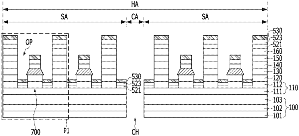
a substrate including a penetrating area and a separating area surrounding the penetrating area, the penetrating area including a substrate hole;
a first buffer layer including a first-buffer lower layer on the substrate, and a first-buffer upper layer on the first-buffer lower layer;
a first thin film transistor on the first-buffer upper layer, the first thin film transistor including a first semiconductor pattern, a first gate electrode, a first source electrode and a first drain electrode, the first semiconductor pattern including poly-silicon, the first gate electrode overlapping with the first semiconductor pattern under a condition that a first gate insulating film is interposed between the first gate electrode and the first semiconductor pattern, the first source electrode and the first drain electrode connected to the first semiconductor pattern;
a second thin film transistor including a second semiconductor pattern, a second gate electrode, a second source electrode and a second drain electrode, the second semiconductor pattern including an oxide semiconductor, the second gate electrode overlapping with the second semiconductor pattern under a condition that a second gate insulating film is interposed between the second gate electrode and the second semiconductor pattern, the second source electrode and the second drain electrode connected to the second semiconductor pattern; and
a separation structure in the separating area of the substrate, the separation structure including a first separation layer having a same stacked structure as the first-buffer upper layer, a second separation layer having a same stacked structure as the first gate insulating film, and a third separation layer having a same stacked structure as the first gate electrode,
wherein the third separation layer which is an uppermost layer of the separation structure, has a greater width than each of the first separation layer and the second separation layer.
|