| CPC H01L 27/14687 (2013.01) [H01L 27/1464 (2013.01); H01L 27/14632 (2013.01); H01L 27/14636 (2013.01); H01L 27/14638 (2013.01); H01L 27/14645 (2013.01); H01L 27/14683 (2013.01); H01L 27/14689 (2013.01); H01L 23/481 (2013.01); H01L 23/525 (2013.01); H01L 24/83 (2013.01); H01L 27/14623 (2013.01)] | 20 Claims |
|
1. A device comprising:
a semiconductor substrate having a frontside surface an opposing backside surface and a sidewall surface extending from the frontside surface to the backside surface;
a plurality of pixel regions disposed in the substrate, the plurality of pixel regions including a first pixel and a second pixel;
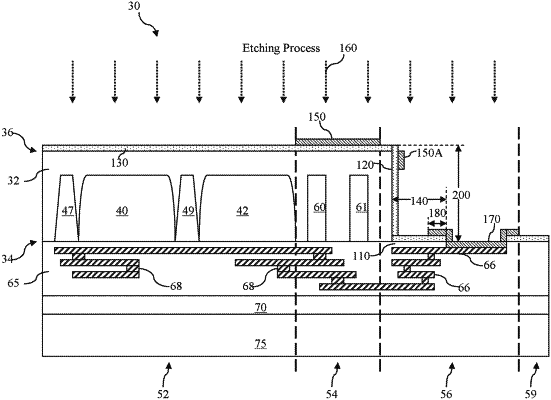
an insulating layer disposed on the frontside surface of the substrate;
a bonding pad disposed on the insulating layer;
a material layer that includes an oxide material disposed on the backside surface of the semiconductor substrate such that the oxide material physically contacts the backside surface of the semiconductor substrate, wherein the semiconductor substrate defines a first opening for partially exposing a backside surface of the bonding pad and the material layer extends along an inner side surface of the first opening defined by the substrate;
a conductive material layer disposed on the backside surface and the sidewall surface of the substrate, wherein no portion of the conductive material layer disposed on the backside surface of the substrate is disposed directly over the first pixel such that no portion of the first pixel is covered by the conductive material layer, wherein the conductive material layer disposed on the backside surface of the substrate is disposed directly over the second pixel such that the second pixel is covered by the conductive material layer.
|