| CPC H01L 27/14685 (2013.01) [H01L 27/1463 (2013.01)] | 8 Claims |

|
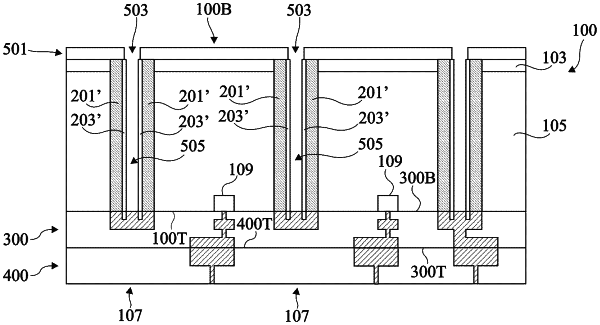
1. Method of forming an insulation structure inside and on top of a first semiconductor substrate, comprising the steps of:
a) forming a trench vertically extending in the first substrate from a first surface of the first substrate;
b) filling the trench, from the first surface of the first substrate, with a polysilicon region;
c) thinning the first substrate on the side of a second surface of the first substrate, opposite to the first surface, to expose the polysilicon region at the bottom of the trench;
d) removing the polysilicon region from the second surface of the first substrate; and
e) filling the trench, from the second surface of the first substrate, with a metal the method further comprising:
between step a) and step b), a step of forming of a first electrically-insulating layer on the lateral walls and the bottom of the trench; and
between step a) and the step of forming of the first electrically-insulating layer, a step of deposition of a polysilicon layer coating the lateral walls and the bottom of the trench.
|