| CPC H01L 27/14649 (2013.01) [H01L 27/1463 (2013.01); H01L 27/14623 (2013.01); H01L 27/14625 (2013.01); H01L 27/14636 (2013.01); H01L 27/14689 (2013.01); H01L 27/14698 (2013.01); G01S 7/4816 (2013.01)] | 20 Claims |
|
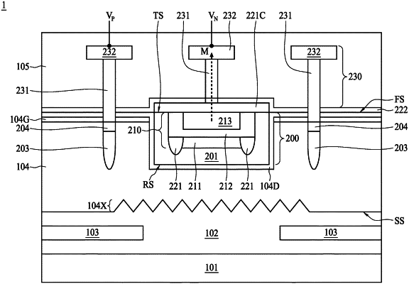
1. A semiconductor structure, comprising:
a substrate comprising a first material, wherein the first material generates electrical signals from radiation within a first range of wavelengths;
an image sensor element comprising a second material, wherein the second material generates electrical signals from radiation within a second range of wavelengths, the second range is different from first range;
a first heavily doped region laterally surrounding the image sensor element;
a transparent layer proximal to a light receiving surface of the image sensor element, wherein the transparent layer is transparent to radiation within the second range of wavelength; and
an interconnect structure connected to a signal transmitting surface of the image sensor element.
|