US 11,901,390 B2
Semiconductor device
Yu-Chien Ku, Tainan (TW); Huai-Jen Tung, Tainan (TW); Keng-Ying Liao, Tainan (TW); Yi-Hung Chen, Kaohsiung (TW); Shih-Hsun Hsu, New Taipei (TW); and Yi-Fang Yang, Tainan (TW)
Assigned to Taiwan Semiconductor Manufacturing Company, Ltd., Hsinchu (TW)
Filed by Taiwan Semiconductor Manufacturing Company, Ltd., Hsinchu (TW)
Filed on Nov. 15, 2021, as Appl. No. 17/525,968.
Application 17/525,968 is a continuation of application No. 16/403,638, filed on May 6, 2019, granted, now 11,177,308.
Application 16/403,638 is a continuation of application No. 15/884,393, filed on Jan. 31, 2018, granted, now 10,283,548, issued on May 7, 2019.
Claims priority of provisional application 62/583,408, filed on Nov. 8, 2017.
Prior Publication US 2022/0077217 A1, Mar. 10, 2022
This patent is subject to a terminal disclaimer.
Int. Cl. H01L 29/40 (2006.01); H01L 23/52 (2006.01); H01L 23/48 (2006.01); H01L 27/146 (2006.01); H01L 23/00 (2006.01)
CPC H01L 27/14636 (2013.01) [H01L 24/05 (2013.01); H01L 27/14643 (2013.01); H01L 2224/0214 (2013.01); H01L 2224/0345 (2013.01); H01L 2224/03831 (2013.01); H01L 2224/0557 (2013.01); H01L 2224/05559 (2013.01); H01L 2224/05567 (2013.01); H01L 2224/05571 (2013.01); H01L 2224/05578 (2013.01)] 20 Claims
OG exemplary drawing
 
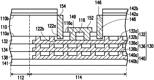
1. A semiconductor device, comprising:
a substrate comprising a first surface and a second surface opposite to the first surface;
a dielectric layer at the first surface of the substrate, the substrate being disposed between the dielectric layer and the second surface of the substrate;
a plurality of dielectric patterns on the dielectric layer and between the first surface and the second surface of the substrate; and
a conductive pad, inserted between the plurality of dielectric patterns and extended into the dielectric layer, wherein the plurality of dielectric patterns are separated from the substrate by a lateral distance.