| CPC H01L 27/1463 (2013.01) [H01L 21/76224 (2013.01); H01L 27/14621 (2013.01); H01L 27/14627 (2013.01); H01L 27/14683 (2013.01)] | 20 Claims |
|
1. A semiconductor device, comprising:
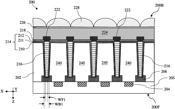
a semiconductor layer comprising a first surface and a second surface opposing the first surface;
a plurality of dielectric isolation features disposed within the semiconductor layer and adjacent the first surface of the semiconductor layer;
a plurality of metal isolation features extending from the second surface of the semiconductor layer;
a metal grid disposed directly over and in contact with the plurality of metal isolation features;
a plurality of microlens features disposed over the metal grid; and
a first dielectric layer extending continuously along the second surface of the semiconductor layer, between the semiconductor layer and the plurality of metal isolation features, and between each of the plurality of metal isolation features and one of the plurality of dielectric isolation features.
|