| CPC H01L 27/14616 (2013.01) [H01L 27/1463 (2013.01); H01L 27/14614 (2013.01); H01L 27/14636 (2013.01); H01L 27/14643 (2013.01); H01L 27/14683 (2013.01); H01L 21/823412 (2013.01); H01L 21/823807 (2013.01); H01L 29/4236 (2013.01); H01L 29/78642 (2013.01)] | 19 Claims |

|
1. A method of manufacturing a transistor of an image sensor, comprising:
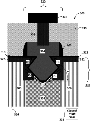
forming a recess to a first depth in a substrate material, the recess corresponding to a gate region and extending in a channel length direction and a channel width direction that is perpendicular to the channel length direction;
forming a trench structure in the substrate material by enlarging the recess to using an isotropic process such that the trench structure extends to a second depth, wherein a width of the trench structure changes from the first depth in the substrate material into the second depth of the substrate material, wherein the trench structure has a polygonal cross section defined in a channel width plane with at least four sidewall portions of the substrate material;
forming a photodiode in the substrate material adjacent to the trench structure;
forming an isolation layer on the substrate material;
forming a gate portion of the isolation layer on the substrate material such that the gate portion of the isolation layer extends into the trench structure; and
forming a gate on the isolation layer such that the gate extends into the trench structure.
|