| CPC H01L 27/1244 (2013.01) [H01L 24/95 (2013.01); H01L 25/167 (2013.01); H01L 27/1259 (2013.01); H01L 24/24 (2013.01); H01L 33/44 (2013.01); H01L 2224/24051 (2013.01); H01L 2224/24147 (2013.01); H01L 2224/95101 (2013.01); H01L 2224/95133 (2013.01)] | 20 Claims |
|
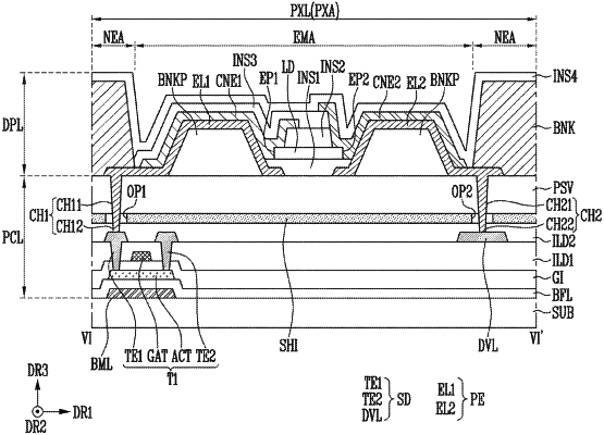
1. A display device comprising:
a substrate;
a first interlayer insulating layer on the substrate;
a data conductor on the first interlayer insulating layer;
a passivation layer on the data conductor;
a pixel electrode layer on the passivation layer; and
a shielding electrode between the data conductor and the pixel electrode layer, and defining a first contact opening and a second contact opening,
wherein the data conductor and the pixel electrode layer are electrically coupled to each other in each of the first contact opening and the second contact opening.
|