| CPC H01L 27/1244 (2013.01) [G02F 1/136286 (2013.01); G02F 1/167 (2013.01); H01L 27/1225 (2013.01); H01L 27/1259 (2013.01); H01L 29/66969 (2013.01); H01L 29/7869 (2013.01); G02F 1/136295 (2021.01); G02F 2201/121 (2013.01); G02F 2201/123 (2013.01)] | 8 Claims |
|
1. An electrophoretic display device, comprising:
an active array substrate, comprising:
a first substrate; and
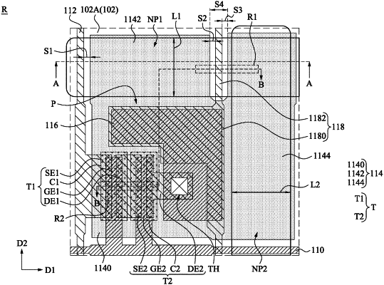
a plurality of pixel structures disposed on the first substrate, the pixel structures being arranged in rows and columns, each of the pixel structures comprising:
a scan line disposed on the first substrate and extending along a first direction;
a data line disposed on the first substrate and extending along a second direction, the first direction crossing the second direction, the data line and the scan line defining a pixel region, a first cutting clearance region, and a second cutting clearance region, the first cutting clearance regions of first ones of the pixel structures in a same row being connected to form a first continuous cutting clearance region spanning the first ones of the pixel structures in the same row, the second cutting clearance regions of second ones of the pixel structures in a same column being connected to form a second continuous cutting clearance region spanning the second ones of the pixel structures in the same column, and the first continuous cutting clearance region being perpendicular to the second continuous cutting clearance region;
a pixel electrode disposed on the first substrate and including a first portion and a second portion, wherein the first portion is on the pixel region, the second portion is on the first cutting clearance region, and a normal projection of the second portion onto a top surface of the first substrate does not overlap a normal projection of the data line onto the top surface of the first substrate;
a common electrode having a main portion and an elongated portion extending along the second direction along which the data line extends, wherein when viewed in a cross section cutting through the second portion of the pixel electrode, the elongated portion of the common electrode and the data line, the common electrode non-overlaps the pixel electrode, and when viewed in a top view, the second portion of the pixel electrode has a terminated edge non-overlapping the common electrode, the common electrode is covered by the pixel electrode in the pixel region;
at least one insulator layer disposed between the common electrode and the pixel electrode, wherein the common electrode, the at least one insulator layer and the pixel electrode are stacked from bottom to top in sequence; and
a transistor electrically connected to the scan line and the data line, wherein the transistor is at a region non-overlapping the first continuous cutting clearance region and the second continuous cutting clearance region;
a transparent electrode layer over the plurality of pixel structures;
microcapsules between the transparent electrode layer and the plurality of pixel structures; and
a second substrate over the transparent electrode layer, wherein the second substrate is a transparent.
|