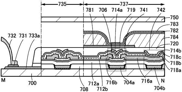
| CPC H01L 27/124 (2013.01) [H01L 21/76849 (2013.01); H01L 27/1255 (2013.01); H01L 29/66742 (2013.01); H01L 29/66969 (2013.01); H01L 29/7869 (2013.01); H01L 29/78603 (2013.01); H01L 29/78609 (2013.01); H01L 29/78648 (2013.01); H01L 29/78654 (2013.01); H01L 23/53223 (2013.01); H01L 23/53238 (2013.01); H01L 23/53266 (2013.01)] | 4 Claims |

|
1. A semiconductor device comprising:
a stack of plurality of insulating films, a first conductor, a second conductor, a third conductor, a fourth conductor, and a fifth conductor,
wherein the stack of the plurality of insulating films comprises a first opening,
wherein the second conductor is provided under the stack of the plurality of insulating films,
wherein the first conductor is in contact with the second conductor at a bottom of the first opening,
wherein the third conductor is provided in the stack of the plurality of insulating films,
wherein the fourth conductor is provided over the stack of the plurality of insulating films,
wherein the first conductor is in contact with a side surface of the third conductor,
wherein the first conductor is in contact with the fourth conductor,
wherein the first conductor is not in contact with the fifth conductor,
wherein the stack of the plurality of insulating films comprises a first insulating film, a second insulating film, and a third insulating film,
wherein the second insulating film has a region which is in contact with a top surface of the first insulating film, and a region which is in contact with a first side surface of the fifth conductor, and
wherein the third insulating film has a region which is in contact with a top surface of the second insulating film, a region which is in contact with a second side surface of the fifth conductor, and a region which is in contact with a top surface of the fifth conductor.
|